In the manufacturing and processing of liquid crystal displays, red and blue mura defects in TFT-LCDs have always been a major defect in module processing.
With the increase in panel size, reduction in glass thickness, improvement in resolution, and optimization of transmittance, the probability of this problem occurring in the back-end module manufacturing process has significantly increased.
More importantly, once red and blue mura defects are formed, they are difficult to repair, directly affecting the panel's yield rate and product reliability.
This article will delve into the definition, phenomena, generation mechanism, and targeted improvement strategies for red and blue mura defects in TFT-LCD screens. We hope this article will provide some assistance to those in the liquid crystal display industry.

Definition Of TFT-LCD Red And Blue Spot Phenomenon
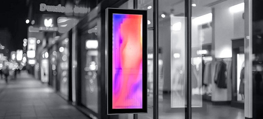
TFT-LCD red and blue spots are a common display anomaly, referring to the appearance of red spots, blue spots, or interwoven red and blue color patches in localized areas of the panel, usually in irregular patterns or with color deviations.
Specifically, when external force is applied to the panel (especially pressure in the Z-axis direction or shear force in the X-axis direction), the internal support structures (Photo Spacers, or PS) will be displaced.
PS are divided into Main PS (main support) and Sub PS (auxiliary support), whose function is to maintain uniform cell gap thickness. When the external force exceeds the design threshold, the PS will slide horizontally, scratching the underlying polyimide alignment layer (PI layer).
The PI layer is responsible for the initial orientation of liquid crystal molecules. Once scratched, its anchoring ability is lost, leading to uncontrolled alignment of liquid crystal molecules in that area. In the normally black display mode (such as IPS technology), this damage manifests as localized light leakage, which appears as red or blue patches to the human eye.
")
This defect is particularly noticeable against a black background and can even be observed in the absence of voltage, directly affecting image uniformity and user experience.
Unlike other reversible defects, red and blue splotches, once formed, are often irreparable, stemming from internal structural damage caused by external mechanical stress.
The Common Red And Blue Blotch Phenomenon In TFT-LCD Displays.
TFT-LCD Monochromatic Spot Phenomenon
When the panel is subjected to combined forces in the Z-direction (vertical) and X-direction (horizontal), the main support column (Main PS) will simultaneously compress and slide towards the non-black matrix (BM) area.
This sliding can scratch the PI layer, damaging its anchoring ability for liquid crystal molecules. In IPS (normally black) mode, this leads to pixel light leakage, forming a single colored spot.
The key point is the amount of deformation: If the deformation of the Main PS is less than the height difference between it and the sub-support column (Sub PS), only the Main PS damages the PI layer, resulting in only a single colored spot.
The type of color spot (red or blue) depends on the direction of sliding—for example, sliding towards a specific pixel sub-area may favor red.
Industry data shows that this situation often occurs in scenarios involving light pressure, such as localized stress caused by improper manual handling.

TFT-LCD Module Multi-Color Spot Phenomenon
Once the mechanism of one type of color spot defect is understood, the mechanisms of other types of color spot defects become easier to understand.
When the external force increases further, and the deformation of the Main PS exceeds the height difference between it and the Sub PS, both will come into contact and scratch the PI layer.
Since the number of Sub PS is usually greater than that of the Main PS, there are more damaged points, so multiple patches of different colors may appear simultaneously on the screen, with a wider distribution range and a more complex phenomenon.

External Factors Affecting Red And Blue Mura Occurrence
The inherent trends in panel design objectively increase the risk of red and blue mura:
○Larger Size: Increased area increases the probability of the panel being subjected to uneven external forces during manufacturing.
○Thinner Design: The glass substrate thickness is reduced to 0.15–0.25mm or even lower, decreasing structural rigidity.
○High Transmittance Design: Reducing the number of pixels to increase brightness lowers the internal support density.
○High Resolution Trend: The black matrix width is reduced, weakening its ability to block light leakage.
Balancing these design goals with reliability is one of the core challenges in contemporary panel engineering.
Solutions To Address Red And Blue Discoloration Issues In LCD Panels
Based on mechanistic analysis, the improvement strategies focus on two dimensions: enhancing the intrinsic pressure resistance of the panel and optimizing process measures to prevent extrusion damage.
The following countermeasures are all derived from actual production verification and can be directly applied to LCD panel production lines.
Enhance The Pressure Resistance Of The LCD Panel Itself
Using High-strength Glass
This can be solved by using glass substrates from brands and materials with higher strength, but it will increase the cost of the LCD display panel itself.
Optimizing PS Density
Increasing the number of Main PS and Sub PS per unit area can disperse stress, but a balance with transmittance needs to be maintained.
Introducing Standardized Testing
Using the "LCD compression test" as a quality control measure, monitoring for color defects, light leakage, or unevenness under a uniform pressure of 60N.

Estandardizing The Operating Procedures For Preventing LCD Panel Damage
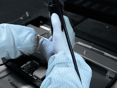
Throughout the entire manufacturing process of LCD back-end modules, there are numerous steps and stages that involve direct contact with the LCD display panel.
If these critical steps and stages are not properly controlled, the risk of red and blue blemishes appearing on the LCD is very high.
a. LCD Breaking Process
During the LCD breaking process, incorrect finger placement (pressing on the LCD display area) increases the risk of red and blue spots appearing on the LCD.
It is generally recommended that during the LCD breaking process, operators only apply pressure along the cutting line, avoiding contact with the display area, to reduce the probability of red and blue spots occurring.

b. LCD Patching And Bonding Process
During the patching process, precisely control the insertion depth, pressure, and speed to avoid excessive compression. For commercial large screens, it is recommended to use automated equipment to monitor these parameters.
In the bonding process, when using a hard-to-hard bonding method, optimize the pressure, time, and vacuum level. Simultaneously, ensure the platform is flat and free of foreign objects. Regular cleaning and calibration of the platform are essential maintenance steps.
c. Handling And Transfer Methods For LCD Products
When transferring LCD panels, the way the operator holds the panel directly affects safety. It is recommended to hold the panel by its two longer sides, avoiding contact with the display area and preventing fingers from pressing on the LCD display area, which can lead to red and blue spots on the LCD screen.
Conclusion
Although the red and blue mura phenomenon in TFT-LCDs is common and difficult to resolve, its occurrence can be significantly reduced through material optimization, process control, and testing and monitoring.
For LCD panel manufacturers, it is recommended to establish a "Red and Blue Mura Improvement Team," integrating R&D, process engineering, quality control, and production departments. This team should conduct root cause analysis of past defective cases and incorporate the findings into design specifications and operating standards.
Only by embedding preventive measures into every manufacturing stage can manufacturers ensure the long-term reliability of their products in real-world usage environments while simultaneously pursuing the limits of display performance.